








By Shane Snider | August 31, 2026
Data Center Knowledge
Executive Overview
In a strategic shift that redefines its positioning within the artificial intelligence hardware ecosystem, Nvidia has announced it is opening its proprietary rack-scale AI infrastructure to custom accelerators developed by hyperscalers and third-party silicon designers. For years, Nvidia’s high-speed NVLink interconnect technology remained strictly locked within its own ecosystem, serving as the proprietary glue that bound its dominant graphics processing units (GPUs) into dense, high-performance computing clusters.
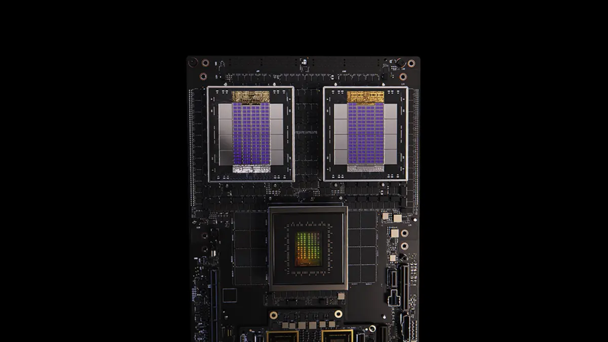
Today, that barrier is coming down. Through an expanded partnership with MediaTek—bolstered by a massive $3.5 billion convertible bond investment from Nvidia—the company is enabling customers to design custom AI accelerators, or XPUs, on a pre-validated platform known as NVLink Fusion. These custom chips can then be directly integrated into Nvidia-connected AI factory infrastructure built around the Modular GPU Accelerated (MGX) server and rack reference architecture.
This move addresses a fundamental reality of the modern data center market: hyperscalers are no longer solely reliant on merchant silicon. Major cloud providers—including Amazon Web Services (AWS) with its Trainium and Inferentia lines, Google with its Tensor Processing Units (TPUs), and Microsoft with its Maia accelerators—have invested billions in proprietary silicon optimized for specific machine learning workflows. Rather than treating these custom processors as competitive threats to be locked out, Nvidia is pivoting to become the foundational infrastructure layer for all high-performance AI silicon.
"Ultimately, this gives customers more freedom to innovate without having to rebuild the entire AI factory around custom silicon," said Dion Harris, senior director of HPC and AI hyperscale infrastructure solutions at Nvidia, during a media briefing.
This comprehensive report examines the mechanics of the NVLink Fusion platform, the financial and strategic depth of the MediaTek partnership, the intensifying architectural battle between proprietary interconnects like NVLink and open standards like UALink, and what this means for the future of heterogeneous AI data centers.
Detailed Chronology: The Evolution of NVLink Fusion and Custom Silicon Integration
To understand the magnitude of Nvidia’s current announcement, it is necessary to trace the incremental opening of the company’s architecture over the past several years:
- May 2025: Nvidia officially unveils the concept of NVLink Fusion, initially signaling an openness to working with third-party silicon providers and CPU vendors to integrate high-speed interconnects into specialized environments.
- Late 2025 – Early 2026: A wave of silicon and infrastructure heavyweights—including Astera Labs, Marvell, Samsung, and AIchip—announce support for NVLink Fusion for custom silicon applications. Simultaneously, CPU architects such as Arm, Intel, Qualcomm, and SiFive signal CPU-side integration compatibility.
- July 2026: Industry analysts highlight a growing bifurcation in data center hardware as inference workloads surge, forcing data center operators to embrace heterogeneous compute architectures that blend GPUs, CPUs, and custom ASICs.
- August 31, 2026: Nvidia drops a bombshell announcement: it is formally expanding its rack-scale AI infrastructure to custom accelerators via an expanded MediaTek partnership, underscored by a $3.5 billion convertible bond investment in the Taiwanese chip designer. Concurrently, competitors like AMD double down on open-standard alternatives like UALink within platforms like the Helios rack system.
Supporting Context & Metrics: The Mechanics of Heterogeneous AI Infrastructure
The transition toward heterogeneous AI infrastructure is not merely a design preference; it is an economic and physical necessity dictated by the physics of modern data centers. As large language models (LLMs) scale into parameters numbering in the trillions, training and inference workloads demand unprecedented bandwidth, low latency, and power efficiency.
The Scale-Up Challenge: Ethernet vs. NVLink Fusion vs. UALink
According to Matt Kimball, vice president and principal analyst at Moor Insights & Strategy, the industry has effectively consolidated around three primary fabric options for connecting processors within large-scale AI systems:
- Scale-Up Ethernet: The traditional, battle-tested networking approach long used in standard enterprise data centers. While highly flexible, it traditionally struggled to match the ultra-low latency required for tight GPU-to-GPU memory pooling.
- NVLink Fusion: Nvidia’s proprietary high-performance scale-up technology. It leverages NVLink-C2C (Chip-to-Chip) links, high-bandwidth memory (HBM) integration, and advanced chiplet packaging to achieve extreme interconnect bandwidth within a rack.
- UALink (Ultra Accelerator Link): An emerging open standard championed by a consortium of competing chip and infrastructure giants—including AMD—designed to provide a non-proprietary alternative for connecting accelerators at scale.
"These fabrics are to make scale-up easier and more performant," Kimball explained. "All require broad ecosystem support to be meaningful."
Inside the MediaTek Partnership and Nvidia’s Financial Commitment
The partnership with MediaTek provides the operational backbone for this strategy. While Nvidia supplies the underlying connectivity, networking, and rack-scale architecture, MediaTek brings world-class system-on-chip (SoC) design, advanced packaging capabilities, and robust manufacturing relationships.
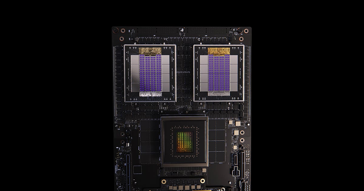
Crucially, Nvidia’s $3.5 billion investment in MediaTek convertible bonds cements a long-term strategic alignment. Production-grade AI factories require sophisticated packaging, HBM integration, high-speed I/O, and rigorous rack-scale thermal and electrical certification. MediaTek will provide the SoC design and packaging expertise for custom XPU customers, while Nvidia ensures that those finished accelerators can plug seamlessly into the MGX ecosystem.
Furthermore, the collaboration extends far beyond the hyperscale data center. MediaTek and Nvidia continue to co-develop local AI computing ecosystems, including upcoming RTX Spark and DGX PC client platforms, as well as next-generation automotive systems that pair MediaTek’s automotive platforms with Nvidia’s AI and graphics stack.
Official Statements and Industry Perspectives
Nvidia’s leadership insists that the decision to open its architecture is rooted in pragmatic systems engineering rather than altruism. The goal is to ensure that no matter what compute engine an enterprise or hyperscaler deploys, the surrounding data center infrastructure—from rack power and liquid cooling to scale-up switches—bears the Nvidia hallmark.
"We’ve built out this incredible ecosystem, which is what we call MGX, that now all these customers can tap into, and they don’t have to go and reinvent the wheel."
— Dion Harris, Senior Director of HPC and AI Hyperscale Infrastructure Solutions, Nvidia
Harris emphasized that customers must maintain the freedom to innovate on compute without being forced to rewrite their entire facility architecture.
"Customers can focus on differentiated compute… It’s really about being able to take all the technologies that we’ve built over the last several decades, and offering that to the ecosystem."
However, market analysts point out that Nvidia’s strategy is also a defensive masterstroke against rising open standards. As competitors rally behind architectures like AMD’s Helios platform—which pairs 72 AMD MI455X accelerators with Epyc CPUs and Pensando networking using the open UALink standard—Nvidia must ensure its proprietary fabric remains the de facto gold standard for high-end AI clusters.
Even major hyperscalers building their own silicon are finding it impossible to completely divorce themselves from Nvidia’s technological gravity. Harris noted that Amazon Web Services (AWS), despite fielding its own Trainium and Inferentia processors, plans to incorporate Nvidia infrastructure technologies—including NVLink-C2C and NVLink switch technology—into parts of its hybrid deployments.
Future Outlook: The Battle for the AI Factory Architecture
As the data center industry looks toward the remainder of the decade, the definition of an "AI factory" is undergoing a profound metamorphosis. The era of homogeneous, single-vendor clusters is giving way to complex, multi-architecture environments where training clusters, real-time inference nodes, and specialized database accelerators must coexist within the same liquid-cooled rack.
Nvidia’s gambit with NVLink Fusion creates a fascinating paradox: by opening its proprietary interconnect to custom silicon, Nvidia is simultaneously mitigating the threat of proprietary hyperscaler chips while tightening its grip on the overarching data center infrastructure stack. Whether customers choose Nvidia’s own Blackwell/Rubin architectures or design custom XPUs via MediaTek, Nvidia stands to monetize the switches, the C2C links, the MGX rack specifications, and the scale-out networking fabrics (Spectrum-X Ethernet and InfiniBand) that hold the entire facility together.
The ultimate test for NVLink Fusion will be adoption velocity. While the roster of participating silicon designers—including Astera Labs, Marvell, Samsung, AIchip, and now MediaTek—is formidable, the gravitational pull of open standards like UALink will test whether developers prefer the absolute performance of proprietary vertical integration or the architectural freedom of open-source interconnects.
One thing is certain: the walls of the walled garden have been fitted with gates. How the broader semiconductor and cloud computing industries navigate those gates will dictate the shape of AI infrastructure for the next ten years.