








By Shane Snider | August 31, 2026
4-minute read
Executive Overview
In a strategic evolution that could reshape the landscape of high-performance computing (HPC) and artificial intelligence infrastructure, Nvidia has announced it is opening its proprietary rack-scale AI architecture to custom accelerators developed by hyperscalers and third-party silicon designers.
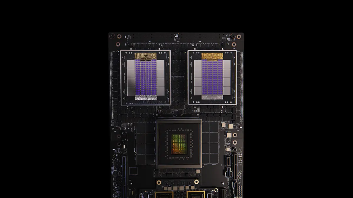
At the center of this pivot is an expanded partnership with chip design giant MediaTek, underscored by a massive $3.5 billion Nvidia investment in MediaTek convertible bonds. By integrating Nvidia’s cutting-edge NVLink connectivity into a pre-validated framework known as NVLink Fusion, the collaboration allows customers to design custom AI accelerators—often referred to as XPUs—that seamlessly plug into Nvidia’s Modular GPU Accelerated (MGX) infrastructure.
This move addresses a fundamental tension in modern cloud infrastructure: while major cloud service providers (hyperscalers) increasingly desire proprietary silicon tailored to specific workloads—such as AWS Trainium and Inferentia, Google Tensor Processing Units (TPUs), and Microsoft Maia accelerators—they have historically been forced to choose between building isolated alternative stacks or buying standard Nvidia hardware.
Nvidia’s new strategy offers a middle ground. By making custom silicon interoperable with its rack-scale stack, Nvidia is positioning itself not merely as a GPU vendor, but as the foundational architecture provider for the entire AI economy. However, this move also arrives amid intense competition from open-standard interconnect alternatives like UALink, setting the stage for a high-stakes battle over how future data centers are connected.
Detailed Chronology & Strategic Shifts
The journey toward an open-architecture Nvidia ecosystem has accelerated rapidly over the last year, driven by the explosive demand for diverse AI workloads, particularly inference, which requires specialized, cost-effective computing.
May 2025: The Genesis of NVLink Fusion
Nvidia first introduced NVLink Fusion in May 2025 as a tactical response to the modular chiplet revolution. Recognizing that monolithic dies were reaching physical manufacturing limits, Nvidia began enabling high-bandwidth, low-latency inter-chip communication standards. Initially targeted at select partners, the platform was designed to marry Nvidia’s high-speed scale-up connectivity with external system-on-chip (SoC) designs.
Summer 2026: Broadening the Ecosystem
Throughout the summer of 2026, the roster of companies aligning with NVLink Fusion expanded steadily. Industry heavyweights like Astera Labs, Marvell, Samsung, and AIchip joined the fold to support custom silicon integrations utilizing NVLink Fusion. Meanwhile, CPU architectures from companies such as Arm, Intel, Qualcomm, and SiFive announced various forms of support on the processor side.
August 2026: The MediaTek Blockbuster and the $3.5B Bet
The definitive turning point arrived on Monday, August 31, 2026. Nvidia formalized its deeper alignment with MediaTek through an expansive strategic partnership and a staggering $3.5 billion investment in MediaTek convertible bonds.
During a media Q&A session addressing the announcement, Dion Harris, senior director of HPC and AI hyperscale infrastructure solutions at Nvidia, laid out the core philosophy driving the company’s new posture:
"Ultimately, this gives customers more freedom to innovate without having to rebuild the entire AI factory around custom silicon."
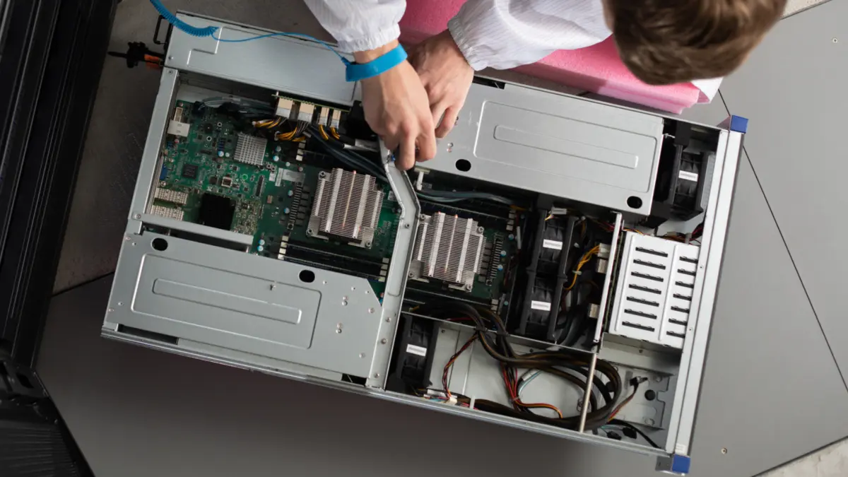
Under this agreement, MediaTek will provide world-class SoC design, advanced packaging capabilities, and high-bandwidth memory (HBM) integration for custom XPU customers. Meanwhile, Nvidia provides the foundational connectivity, networking fabric, and rack-scale blueprint via its MGX ecosystem.
Supporting Context & Industry Metrics
To fully understand the gravity of Nvidia’s strategy, one must examine the shifting economics of modern data centers. Hyperscalers spend tens of billions of dollars annually on custom silicon. Designing a custom AI accelerator allows these tech giants to optimize price-to-performance metrics for specific deep learning models.
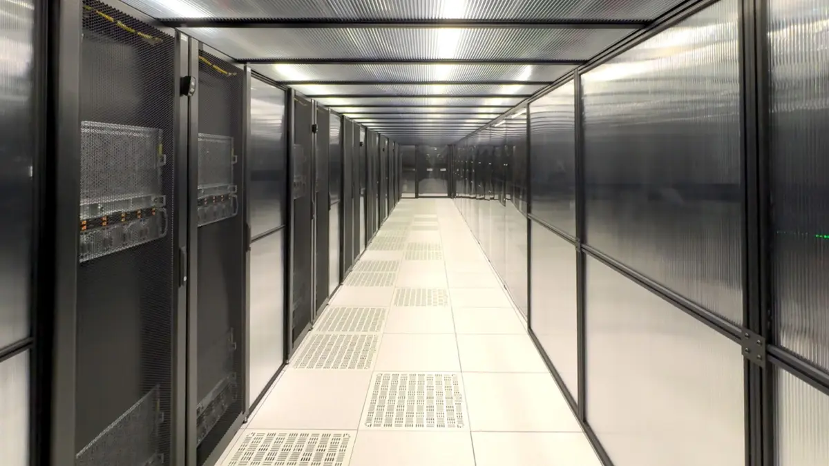
However, building custom silicon is only half the battle; the real engineering bottleneck lies at the rack scale. As clusters scale to tens of thousands of accelerators, packaging, HBM integration, input/output (I/O) management, and multi-node networking become immense hurdles.
The Tripartite Battle for Scale-Up Fabrics
As heterogeneous AI infrastructure becomes the industry norm, analysts note that the market is coalescing around three primary scale-up methodologies. Matt Kimball, vice president and principal analyst at Moor Insights & Strategy, highlighted the shifting dynamics:
"Heterogeneity isNOWLEDGE the future of AI. There are effectively three options: Scale-up Ethernet, NVLink Fusion, and UALink. These fabrics are to make scale-up easier and more performant. [All] require broad ecosystem support to be meaningful."
- Scale-Up Ethernet: The traditional, ubiquitous data center networking approach, increasingly bolstered by high-speed iterations like 102.4T Ethernet.
- NVLink Fusion: Nvidia’s proprietary, ultra-high-bandwidth scale-up technology that extends beyond Nvidia’s own GPUs to support custom XPUs and third-party chiplets via NVLink-C2C (Chip-to-Chip) links.
- UALink (Accelerator Link): An open-standard alternative championed by an industry consortium that includes AMD, designed to challenge Nvidia’s proprietary grip on accelerator connectivity.
The Rise of Competing Architectures: AMD’s Helios
The pressure on Nvidia’s proprietary model is very real. Competitors are aggressively fielding open-standard rack-scale solutions. For instance, AMD recently fired back at Nvidia with its Helios AI system, which pairs 72 AMD MI455X accelerators with Epyc CPUs and Pensando networking. Helios leverages UALink for high-speed scale-up connectivity, demonstrating that the industry has viable alternatives if it chooses to reject proprietary lock-in.
Despite these competitive pressures, Nvidia’s reach remains formidable. Even major rivals or customers with competing silicon lines are finding it difficult to ignore Nvidia’s infrastructure footprint. Harris noted during the briefing that Amazon Web Services (AWS)—despite developing its own Trainium and Inferentia processors—plans to utilize a hybrid approach combining its proprietary chips with Nvidia infrastructure, including NVLink-C2C and NVLink switch technology.
Official Statements and Industry Perspectives
Nvidia’s leadership has been careful to frame this pivot not as a retreat from proprietary hardware, but as an expansion of its role as an infrastructure powerhouse.
When pressed on whether Nvidia’s long-term objective is to control AI architecture design regardless of what silicon sits inside the customer’s server rack, Dion Harris pushed back against the narrative of corporate dominance:
"It’s not about ownership. It’s really about being able to take all the technologies that we’ve built over the last several decades, and offering that to the ecosystem."
Harris emphasized that production-grade AI factories require an immense amount of pre-qualification and certification at scale. By leveraging Nvidia’s MGX modular server and rack reference architecture, customers bypass the grueling trial-and-error phase of infrastructure design:
"We’ve built out this incredible ecosystem, which is what we call MGX, that now all these customers can tap into, and they don’t have to go and reinvent the wheel… Customers can focus on differentiated compute."
Analyst Matt Kimball underscored that the success of any fabric—whether it is Nvidia’s proprietary NVLink Fusion or the open-standard UALink—will ultimately be decided by software support and developer adoption:
"These fabrics are to make scale-up easier and more performant. [All] require broad ecosystem support to be meaningful."
Future Outlook: Beyond the Data Center Accelerator
While the immediate focus of the Nvidia-MediaTek partnership centers on data center infrastructure and NVLink Fusion, the scope of their alliance extends far beyond enterprise server racks.
The two companies are actively collaborating on local edge AI computing initiatives, including future RTX Spark and DGX PC client platforms. Furthermore, they are pushing aggressively into the automotive sector, integrating MediaTek’s robust automotive vehicle platforms with Nvidia’s world-class AI and graphics software stacks.
Key Takeaways for the Enterprise and Data Center Operators
- The Death of Monolithic Lock-in: Hyperscalers no longer have to choose between 100% Nvidia hardware and building their own isolated data center architectures. They can now merge custom silicon with Nvidia’s proven interconnect fabric.
- The Licensing Frontier: While precise financial details of the NVLink Fusion licensing model remain opaque, Nvidia has confirmed that commercial licensing elements will be embedded into the framework.
- The Interconnect War Intensifies: The battlelines are officially drawn between Nvidia’s proprietary NVLink Fusion ecosystem and open standards like UALink and Scale-Up Ethernet.
As inference workloads surge and enterprises demand hyper-specialized silicon to manage operational costs, Nvidia’s tactical evolution ensures that even if a data center runs on custom silicon, the underlying highway systems moving the data will likely still bear Nvidia’s stamp.
About the Author
Shane Snider is Senior News Writer at Data Center Knowledge, covering AI infrastructure, hyperscale data centers, cloud platforms, and the power and energy systems driving modern compute expansion. His reporting focuses on the operational, economic, and environmental forces reshaping digital infrastructure, including AI factories, utility constraints, liquid cooling, and next-generation data center architectures. Based in Raleigh, North Carolina, Snider has earned Azbee awards for his investigative news series and government reporting.